
Eddystone LINK, SSDP As well as mDNS Support Physical Web
Intro to the Physical Internet
Signs suitable for all kinds of application scenarios that call for communication between day-to-day things and similarly their setting. The physical web assists consumers make suitable use of the resulting chances. In this post, we will provide simply how does physical net task, and also there's no question that the Eddystone WEB LINK plays a crucial obligation throughout the working of the Eddystone.
In 2014, Google supplied its open-source job Physical Web to connect the digital world a large amount extra thoroughly with the real one. Bus quits, visitor locations, day-to-day factors, or grocery store products-- in concept, each of them can currently independently send messages to smartphones through indications. The basis for such communication is the Bluetooth Low Power (BLE) radio modern-day innovation. If a point has in truth been provided with an indication, it can send messages to smart tools that maintain BLE, for instance signaling concerning hold-ups, special offers, or project days.
In this context, the physical web makes certain, to name a few factors, that individuals do not need to position brand-new applications around, nonetheless can check out the news on a regular user interface. It can be used in mostly all instances in which clients have a rate of interest in information about their arrangement or which interaction in between them, as well as additionally clever points, is required. To get a far much better referral of such circumstances, three brief application circumstances stay with.
Watched on family residence devices: The physical net can additionally be utilized to control along with screen family members' house appliances such as the cleansing gadget. Each device sends a LINK that explains an IP address in addition to can just be gotten to when connected to the neighborhood network. The visibility of the LINK can be restricted to products in the network if network expedition methods such as DNS and likewise SSDP are utilized as opposed to BLE.
Physical internet or single applications
In comparison to numerous other details offers (e.g. routine details or traveler organization), where people call for to mount their application for every and also every supplier, the physical web consists of Eddystone LINK sent out by the signs as if they were a search query on a web site. So customers can find smart factors in their ambiance with just one application, also, to connect straight with them. One more benefit: no favorable notifications are sent. The certain simply see a list of things in his area if he means to.
Together with the BLE, MOKO Smart Bluetooth Beacon, in which the author functions, recommends a strategy for sending in addition to getting Links in neighborhood networks that are based upon the Basic Solution Discovery Approach (SSDP). With the help of SSDP, it is feasible to restrict the visibility of sent out Eddystone INTERNET LINK in local networks along with furthermore, therefore, enhance the link defense.
The Physical Web is readily offered as a work under the Apache accreditation on MOKOSmart in addition to consists of implementations for systems such as Android, iPhone, along with also Node.js. The physical net applications for Android as well as apple iPhone are offered in the Apple Application Store as well as also the Google Play Shop. All applications are to be acknowledged as variations, which permit developers to look into the physical internet at a start. In the future, it ought to certainly be used on many various other mobile phones along with cellphones.
Simply precisely just how does the physical web job?
The physical internet is stated to be an expansion of the web. Like all web technologies, it is open to everyone together with everyone can develop it a lot more. Considered that the system is based upon the display screen of Hyperlinks, it is decentralized in addition to not taken care of by any type of kind of individual. The Eddystone URL can cause very easy details website, to a lot additional detailed, interactive web applications as well as additionally even to indigenous applications. The physical internet methods looking at the internet:
The personal phones a listing of points from his area.
A list of links is presented.
The exclusive choices one.
The WEBLINK appears in the internet browser window.
The abiding by facets must be taken into account from a technological viewpoint:
1. Send comments
2. Background
3. Conserved
4. Location
- Sending as well as obtaining Hyperlinks: There are numerous approaches to send out Links. The physical web presently sustains transmission through BLE, DNS, and SSDP (a whole lot a great deal more on this in the complying with the area).
Obtain fundamental information from websites: The physical web customer develops Links found in addition to sends them along with all important information (e.g. signal durability) to an internet remedy. This, as a result, calls the important info such as the title, recap, in addition to a symbol of the web site in addition to returns the search results page web page to the customer. The prototype application of the net treatment is used in the job's GitHub database.
- Providing the results: A ranking is needed when it worries offering the many URL-sending gadgets from the area. The physical internet customer can organize according to stand for sturdiness, details option in addition to numerous other criteria. The system ought to iron out spam beforehand. Since the net online internet search engine has the same problem, their method can be used for the physical internet. In the results existing, the customer clicks a listing point in addition to the web browser opens the connected website.
- As reviewed, the physical web presently recognizes three methods to send as well as also acquire Hyperlinks. They are based upon 2 various treatments: Bluetooth Low Power along with Network Remedy Exploration. In theory, additional approaches could be included the future. As an instance, programmers can use audio watermarking innovation to install a LINK in an audio signal. In this circumstance, the physical net consumer would need to be widened to be able to acquire audio signals along with analyzing the Links included therein.
Ble Bluetooth in addition to Eddystone
The initial draft of the physical Web USES BLE to send out the LINK to the proper package. The modern technology is truly energy-efficient, particularly if the item using it is run in send setting (non-connectable BLE setting), as when it involves the physical internet. Tiny BLE tools can send out Eddystone RELATE TO a single switch cell for almost 2 years.
An Eddystone message has 2 typical information key in a marketing and advertising data block (ADVERTISEMENT): UUID in addition to details service. Both kinds use a 16-bit commonly distinct identifier (UUID) that abides by the Bluetooth requirements. The UUID service booked for Eddystone is 0xFEAA. It provides a system for reputable, cross-platform history scanning that both Android in addition to similar iPhone authorization. The doing well bytes of the PROMO block has the info certain to the framework. The first byte specifies the structure type. Simply the 4 most significant littles are presently made use of. The 4 reduced ones are scheduled for later usage in addition to furthermore needs to have the worth 0000.
The Eddystone UID structure sends a distinct 16-byte sign ID that includes a 10-byte namespace ID in addition to a 6-byte circumstances ID. Although the namespace ID can be made use of to organize a particular collection of indicators, the circumstances ID helps to acknowledge the devices in the group.
If you think about the principle of the Eddystone UID, it runs in equivalent techniques to the iBeacon presented by Apple in 2013. The iBeacon package has 16 bytes near the UUID, a 2-byte key domain name, as well as a 2-byte added domain. iBeacon packages contain a 16-byte closeness UUID, 2-byte significant in addition to 2-byte small areas. The distance UUID can be utilized to determine an organization or application like a service. Substantial in addition to small fields make it possible for a more comprehensive job of the recognition determined by the UUID, as when it pertains to a branch. Eddystone-TLM is presently sending out telemetric info such as battery standing, tool temperature level as well as the variety of plans sent by the indication.
Network Choice Exploration
Along with BLE indicators together with Eddystone LINK, network exploration approaches such as SSDP in addition to mDNS supply the option of sending Hyperlinks. You can similarly send Links to tools on neighborhood networks. The method has 2 advantages over BLE: First, just clients who are seen to regional networks can see the Hyperlinks, along with 2nd, there is no INTERNET LINK size restraint equivalent to BLE.
Using Network Expedition for the physical internet makes good sense in circumstances where security along with individual privacy plays a crucial function. An instance would be the fantastic house area if access to devices requires to merely be limited to individuals from the precise identical home.
The Basic Option Discovery Approach (SSDP) is a network strategy for advertising in addition to the discovery of services together with devices in neighborhood networks. It develops the exploration layer of the worldwide plug-and-play procedure (UPnP) in addition to likewise assists to market just recently included tools that are defined as control aspects. It likewise permits you to look for tools as well as additional information remedies.
Such characteristics are based upon both sorts of SSDP messages. Originally, there is the promotion message that a gizmo sends out as quickly as it is consisted of in the network. The message to the conventional multicast address as well as additionally port 239.255.255.250:1900 is ssdp: energetic. Control variables bear in mind the port to acquire SSDP messages in addition to consequently to be able to find new tools and also similar services. Before UPnP devices vanish from the network or are no longer used, they need to send the message ssdp: au revoir to the specific same multicast address in addition to similarly the matching port.
Physical Internet sustains SSDP to send out as well as likewise get Hyperlinks in neighborhood networks. Fraunhofer FOKUS created the concept and likewise implementation of the equal system. The application contains the adaptation of SSDP in the physical net application for Android and also apple iPhone for getting Links making use of the technique. Additionally, a cross-platform device based upon Node.js is offered to send out Hyperlinks in a similar way.
When benefiting from SSDP, a physical internet gadget attached to the area network sends out the complying with ssdp: to life message as quickly as it is quickly readily available in the network:
EDUCATE * HTTP/ 1.1 HOST: 239.255.255.250:1900
CACHE-CONTROL: max-age = secs till ad goes out
LOCATION: INTERNET WEB LINK of the internet websites to advertise
NT: container: physical-web-org: device: Fundamental: 1
NTS: ssdp: to life
WEB SERVER: OS/ version UPnP/ 1.0 thing/ variation
USN: promotion UUID
The NOTIFY method in the initial line advises that it is a marketing and advertising message. While the LOCATION header specifies the physical web LINK that is sent out, the NT header defines the product kind, which when it entails the physical net is a container: physical-web-org: tool: Crucial: 1. The ssdp: the energetic well worth of the NTS header recommends that the physical web gadget is readily supplied. Last but not least, the USN header offers a distinct name that can be used to acknowledge the tool. Physical internet clients working on sensible tools or tablet computer systems focus on the multicast address and also port 239.255.255.250:1900 along with also filter the physical net SSDP messages by evaluating the well worth of the NT header. You can after that examine the SSDP message and also have a look at the well worth of the AREA header that lugs the sent out INTERNET LINK.
Physical net gizmos need to send the complying with ssdp: bye-bye message before quitting the network:
ALERT * HTTP/ 1.1 HOST: 239.255.255.250: 1900
NT: container: physical-web-org: tool: Requirement: 1
NTS: ssdp: farewell
USN: promo UUID
ssdp: au revoir makes it clear that the physical internet tool is no more comfortably available from now on. The well worth of the USN header continues to be such in the ssdp: to life message. Physical web consumers that get such a message look for the URL about the USN as well as after that remove it from the checklist.

Thermal conductivity guide for FR4 circuit boards
 FR4 Thermal Conductivity administration for LEDs
Much like the light-emitting diode, which for years offered solely as an indicator lamp, PCB has likewise left its shadowy presence as well as has quickly progressed to a multifunctional element within an electronic system. It, for that reason, has to withstand high currents and guarantee the air conditioning of high-clocked, yet heat-producing CPUs as well as heat-dissipating power parts, which brought us to today's topic- FR4 thermal conductivity.
1. The contrast of a conventional two-board remedy with FR4/ copper mix
As UHB LEDs (Ultra High Brightness LEDs) with as much as 10 or more watts per real estate and also LED varieties with numerous LEDs placed closely next to each other are being made use of increasingly more, the inquiry of warmth dissipation is coming to be an increasing number of press.
This uses specifically given that, unlike incandescent lights, light-emitting diodes just emit a negligible part of the heat loss; virtually everything goes the means of warmth transmission.
Of course, there are solutions, for instance, ceramic carriers or IMS PCB (protected steel substrates) with thick lightweight aluminum cores. Nevertheless, these are costly in comparison to classic FR4 PCB boards, and also a 2nd board is typically needed to make to accommodate motorist electronics.
FR4 PCB with copper cord
Moko Technology takes various methods with "HSMtec". The technology, which is qualified based on DINEN60068-2-14 and JEDECA101-An and also audited for aeronautics and automobile, is careful: only where high currents are supposed to stream via the printed circuit board does thick copper.
Currently, 500µm high profiles with widths from 2.0 mm to 12mm are available in variable lengths, with cables a diameter of 500µm has come to be established. The solid copper components that are securely bonded to the conductor patterns can be used directly to the base copper using ultrasound connection technology and integrated into any kind of layer of a multilayer making use of FR4 base material. There are several reasons why copper is made use of: It has two times the thermal conductivity contrasted to lightweight aluminum and thus makes sure rapid warm dissipation without protecting intermediate layers underneath the LED warmth pad.
Table 1: Thermal conductivity of the products entailed
One more benefit of copper and the motherboard base product FR4 is the thermal development homes (Table 2): Especially about ceramic LEDs, circuit boards based upon copper or FR4 have a high resistance to thermal stress and anxieties, which depend upon environmental or operating problems as well as others Temperature level cycles, such as for "intelligent" lights controls.
Table 2: Thermal expansion coefficient in the X/ Y instructions
In this way, the lifespan as well as reliability of the entire lights device can be considerably increased contrasted to conventional metal core PCB based on aluminum.
Printed circuit boards take care of warm
A look at the specific thermal conductivity shows the relevance of the continuous metallic path from the resource to the sink and the performance possibility of HSMtec. Copper conducts warmth 1000 times much better than FR4. The mix of incorporated copper profiles with modern circuit board constructions such as mini and the movies makes it possible to directly get in touch with a soldering surface area (elements, warm sink) to the profiles, thereby staying clear of bottlenecks in the thermal course.
A thermally maximized layer structure additionally ensures fast heat spreading and also hence sustains the entire thermal concept. In the case of very small LED real estates, filled up microvias make sure a direct metal connection to heat-conducting copper elements, which can be attached roughly 60 μm below the leading layer of the circuit board.
2. Thermal homes of steel core boards and FR4 thermal conductivity with ingrained copper
Contrasted to Thermovias, which are placed directly under warm pads, for example, it is possible to solder loaded microvias with no issues. Based on numerous empirical studies, Häusermann was able to gain all types of knowledge in the locations of thermal management and high current on the published motherboard. The main benefit of HSMtec compared to different remedies is the use of low-cost conventional FR4 material in addition to production in the common production procedure. It is additionally feasible to use this procedure to construct independent, multi-dimensional published motherboard with copper wire
With the help of notch milling at the established bending points, specific segments can be brought right into the wanted orientation by any change of the inclination angle. The thick copper integrated with accounts and cords holds up against currents of up to 500 A. This stands for a practical option to circuit card options that supply full-area copper layers up to 500 µm thick, or to cost-intensive IMS services that use enormous aluminum cores as heat service providers instead of the usual base material deploy.
The layout allows large amounts of warm and/or high currents of approximately 500A to be conducted straight inside the circuit board. Also, the whole style does not call for wires, adapters, or various other mechanical links. This not only raises the integrity of the application but also its lifespan. To effectively implement imaginative lighting design with power LEDs, close participation between the customer and the motherboard producer is essential: Currently, in the concept phase, the whole thermal style-- from the published circuit board to the luminaire real estate-- have to be ideally coordinated. Different model variations and thermal analyzes allow private remedies.
The residential properties as well as qualities of FR4 thermal conductivity materials guarantee wonderful flexibility at an affordable cost. For this reason, they are usually made use of to produce PCB boards. So it is not unusual for us to commit a post to them on our blog site.
FR-4 is a typical set by the NEMA (National Electric Manufacturers Association) for a compound of hard epoxy material as well as fiberglass material. The code 94V-0 gets on all FR-4 motherboard. It guarantees that fire does not spread and heads out once again quickly if the product catches fire. The glass transition temperature level (Tg) for High TG or HiTG is between 115 as well as 200 ° C relying on the manufacturing method and the resins utilized. FR-4 uses bromine, a chemical element, and also a supposed refractory halogen. It replaces G-10, one more composite material that is much less fireproof in many applications. FR-4 also provides an excellent proportion of fire resistance and weight. FR-4 High CTI: The Comparative Tracking Index (tracking resistance) is over 600 volts. FR-4 without copper foil: Preferably fit for insulation boards, versions as well as circuit card service providers. More information concerning the properties of these various materials can be located later in this short article.
What holds our globe with each other
What is "base product"?
The individual components of the typical base material are sticky, a backing product, and also the conductive layer. The FR4, one of the most extensively utilized base product, is made from glue Epoxy material and also the base product constructed from twisted glass fibrils, which are woven right into a glassmaker. "FR" stands for "Flame Retarding" and therefore points to the important fire retardant Residential property of the material. The "4" means a particular FR type. There are additionally the types "FR2" and also "FR3", which are barely in use nowadays, and "FR5" with a higher one Temperature resistance as "FR4".
Prepregs as well as laminates
When producing the FR4 base product, the glass textile with the epoxy resin is made use of initial soaked. The outcome is "Prepregs", an artificial word that stands for "Preimpregnated" as well as on it to indicate that the epoxy resin matrix has dried out yet has not yet set.
Each prepreg consists of precisely one type of glass material, which is specified with a number, for example, "106", "1080", "2116" or "7628". This type of classification was formerly associated with the prepreg density is very binding. The 106 had to do with 50 µm thick, 1080 concerning 60 µm, 2116 approx. 115 as well as the 7628 approx. 180µm.
The modern-day demand for a secure yet likewise affordable pressing of Multilayers has resulted in numerous prepreg variations that vary in the density of the resin finish vary. There are still prepregs with typical material web content but now additionally with medium ones and high resin content. The typical identifiers are after that "SR" for "Criterion resin", "MR" for "Medium resin" as well as "Human Resources" for "High material". Consisting of all producing tolerances, the thickness of one so-called 1080 prepregs just recently in between 56µm (= SR variation, reduced resistance) as well as 84 µm (= HR version, upper resistance) vary.
Colloquially, "slim laminates" with thicknesses between 0.05 mm and 0.86 mm, as well as "Thick laminates" with densities between 0.90 mm and 3.2 mm offered. The density of the copper cladding can be 5, 9, 12, 17, 35, 70, 105, 210, or 420µm. There is no straight physical home connected with these copper thicknesses. The classifications come from the Anglo-American language location for historic reasons simply a several or an integer divisor of 1 ounce (= 35µm). Vincenz, Taube, Wiemers: PCB and also setting up modern technology PCB and setting up technology. Prepregs as well as copper aluminum foils are Electronic devices resources. laminates are currently acquired items. By the way, this recommendation additionally clarifies the classic PCB thickness of 1.50 mm.
Technical qualities of FR4 thermal conductivity
The foreseeable future belongs to the FR4 as well as its derivatives. The product is stable, the insulation is trusted, the dielectric behavior is usable, the prices serve, the processing is developed, and also the heat resistance is bearable. The derivatives are essentially generated by customizing the epoxy material matrix. Following the switch to lead-free electronics (~ RoHS), it has become typical to replace part of the material volume with mineral fillers. This postpones the temperature-related raised Z-axis expansion of the circuit card (parameter CTE (z)="Coefficient of thermal expansion").
As a result of the higher temperature resistance, the probability that the circuit card will be harmed throughout soldering. One after that speaks of "FR4 thermal conductivity with a higher Tg worth" or additionally of "high Tg material". The common value for FR4 is 130 °, higher Tg worths are 150 ° or 175 °, depending upon the product manufacturer. In general, "Tg" is misleadingly equated as "glass transition temperature level". What is indicated, however, is that the epoxy resin framework becomes soft as well as elastic as quickly as the Tg worth is gotten to and that the Z-axis development, as a result, boosts considerably.
Mistake occasions are after that fractures in the called vias and/or tears of the interior conductor tracks from the using sleeves. Delaminations can also occur which results in the partial dissolution of the pressed material compound. The consequence is generally a failure of the component. The continual operating temperature level of a module with FR4 product should not exceed 95 to 100 ° C. A higher Tg worth does not raise the continuous operating temperature of a module. The continual operating temperature essentially relies on the epoxy resin matrix as well as must not exceed 95 to 100 ° for FR4 material. One more parameter is the Td worth. "Td" means "Time to Decay" and also explains the temperature level value at which the product has lost 5% of its mass due to outgassing/evaporation.
Since the introduction of SMD technology, the demands for the base product have raised. The decrease in the design of SMD components additionally results in a decrease in the SMD locations on the circuit board, since or else, reliable soldering is not possible (i.e. twisted elements, tombstoning). When an SMD pad obtains smaller, the location with which this pad abides by the circuit board additionally becomes smaller. Basic mechanical loads, resonance, and braking or acceleration forces can cause the element to rips. Reflow soldering furthermore reduces the attachment between the SMD pad and also the motherboard by approximately 75%, relying on the base product type, circuit board surface area, and the number of reflow cycles. Regrettably, the steps to attain a high Tg in return frequently lead to a reduction in the copper attachment. With common material, pull-off forces of around 2 N/ mm can be discovered, which can drop to 0.8 N/ mm with high-Tg material.
Keep in mind
Find out about the technical quality of base materials online or via a talk to your PCB maker. Utilize the physical residential or commercial properties of Base materials for your circuit principle. Make sure that the made use of base material for constantly high item top quality of MOKO Printed Circuit Board Assembly.

Research on transmission speed of lorawan
The most important ability of IoT devices is that of interaction. there are various methods with different areas of application. While WiFi, Bluetooth, Zigbee, or other radio standards are commonly utilized for brief ranges in the residence, devices have to lie in other places to make use of alternate innovations. Such a group of technologies is MOKO LoRaWAN Gateway. Nevertheless, these have the advantage of a dramatically longer variety and better power effectiveness than the majority of various other radio standards at the cost of bandwidth. The picture listed below shows LoRaWAN contrasted to some other cordless communication methods. LoRaWAN technologies are mainly used when end tools are mounted in locations that only work with various other innovations that are difficult to achieve, or when power performance is of wonderful significance. In this LoRaWAN is used as LPWAN innovation.
Nonetheless, variety and also power intake are not the only important points in the IoT. One issue that is usually neglected is the safety and security of networked gadgets. Between 2017 and 2018 alone, the number of recognized malware for IoT gadgets increased almost quadrupled. But malware isn't the only threat. Lots of IoT gadgets send out data improperly protected, creating attacks on that particular data and hence additionally on the IoT infrastructure. Espionage, adjustment of information, and also the full requisition of systems are exemplary assault circumstances.
One more pertinent topic in IoT security is firmware updates; they allow suppliers to bring new features to devices as well as, in the event of safety occurrences, to fix them without the user having to end up being active. The updates must be additionally performed in a protected manner to make sure that opponents are incapable to infuse phony firmware right into a device.
Integrating firmware updates as well as finish devices that use a LoRaWAN method for data transmission produces a completely brand-new difficulty. While for IP-based innovations, such as B. W-LAN, there are already some tips for particular methods, updates employing LoRaWAN are still mostly uncharted. The factor that the classic methods can not be made use of can be discovered in the limitations of LoRaWAN modern technologies. LoRaWAN, for instance, has high limitations in terms of information price and LoRaWAN transmission speed and has no standardized transportation method, which compensates for losses in information transmission could.
1.1 The smart mailbox
In this job, a detailed application is taken into consideration and also different topics of IoT safety are taken a look at. A clever mailbox was created, which notifies the user employing their smartphone when mail is in the mailbox has been obtained.
1.1.1 Usage situation
The keynote of the smart mailbox is to make sure that the user does not regularly need to open his mailbox to find out if there is any mail in it. Instead, he ought to obtain a notice on his mobile device as soon as there is mail is in the mailbox. This has the advantage that the time of the individual is not unnecessary as a result of mailboxes that are far from the individual or that rarely include mail Is declared.
The features of the application are intentionally maintained tiny due to the concentrate on protection as well as energy performance. Furthermore, the application was developed as an "extension". It ought to be possible to do this with little initiative for the individual to install any type of letterboxes. Battery procedure as well as a little form variable therefore additionally demands the job.
1.1.2 Checked out topics with LoRaWAN transmission
As pointed out earlier, the focus of the job is on IoT security. Furthermore, energy efficiency is thought about. From these concerns, several subtopics are examined utilizing the wise mailbox that has been the first point is the secure, E2E-encrypted data LoRaWAN transmission. Particularly With mailboxes in public locations, it is very important that an assaulter does not learn can establish whether and also just how much mail is in the mailbox. This stops that can quickly learn if a burglary would certainly be worthwhile. Security is likewise important against control to avoid the customer from receiving incorrect info regarding the condition of the mailbox. Furthermore, it is checked out to what degree the settlement of cryptographic tricks for these jobs is a safe and secure means can be performed without the maker of the device or 3rd parties can learn.
The next main point of examination is the safe and secure firmware updates using LoRaWAN. There is presently no official common regarding the transfer of firmware. Updates through LoRaWAN. In this respect, it is one of the major tasks of this job
to make and examine. In the end, the smart mailbox needs to have the ability to perform firmware updates via LoRaWAN without user treatment. These updates need to likewise be cryptographically secured to stop manipulation. Lastly, it is checked out how mail is thrown right into a mailbox device that can be acknowledged. Various innovations were analyzed as well as an ideal one was determined.
2.1 LoRaWAN
LoRaWAN is a LoRaWAN service for IoT applications with a percentage of information energy-efficient and can be transferred wirelessly over large distances. It consists of the one hand of LoRa radio, a method for physical information LoRaWAN transmission and also on the other hand of LoRaWAN itself, a MAC method which is based on LoRa develops and provides a standardized treatment for the transfer of information via LoRa LoRaWAN, as one of the bottom lines in this work, was utilized for interaction with completion gadgets, consisting of the smart mailbox.
2.1.1 What is LoRa.
LoRa is a frequency modulation process developed by Semtech wireless communication between two communication companions permitted. It is, therefore, a physical method (OSI Layer 1), which just takes over the inflection of the physical information transmission. LoRa makes use of frequency-modulated chirps to encode symbols. The chirp inflection utilized uses "chirps" to send signs. The frequency is constantly changed throughout the data transfer over a defined period. The symbols transferred are about the beginning of the chirp are defined.
The main benefits that this modulation provides compared to FSK or PSK are the long-range and also the toughness versus noise. Both are from the spreading element and data transfer utilized. The spreading element identifies for how long a single chirp lasts, ie exactly how wide it is spreading out". A higher aspect suggests broader signs, which guarantees much longer LoRaWAN transmission arrays, yet likewise slower information transmission. In LoRa dispersing elements from 7 to 12 is specified, which indicates LoRaWAN transmission speed from an optimum of 37.5 kbit/ s to a minimum of 300 bit/ s can be achieved. The data transfer is repaired at 125 kHz, 250 kHz or 500 kHz as well as additionally affects the array and also rate of the signal. The concrete choice of these criteria is identified by LoRaWAN
The regularities that LoRa makes use of relying on the area. In Europe, you can 868 MHz or at 433 MHz can be sent out. It is important to mention that these regularities are license-free spectra, so there is no permit fee to utilize them. To compensate for this, apply temporal, send out restrictions that all devices have to follow. These are between 0.1% and also 10%, depending on the frequency utilized.
2.1.2 What is LoRaWAN.
LoRaWAN is a MAC protocol (OSI Layer 2), which is based on LoRa (but additionally with FSK can be used), as well as likewise some components of a network method (OSI Layer 3) consists of. It defines a message format, as well as MAC commands to control the transfer. The parameters for the underlying LoRa transmission are likewise figured out by LoRaWAN. The very first part is the actual requirements, which specify the message formats, the MAC commands, and also the series. The regional specifications, which details setups for LoRa, as well as some changes or additions to the LoRaWAN procedure, are readily available as an expansion define relying on the respective area.
A LoRaWAN network contains numerous groups of individuals as well as is organized in a star-by-star topology, as displayed in Number 5. In the middle is the network web server, which is the server-side administration of the LoRaWAN network as well as uses an API for client applications. Manage LoRaWAN applications and also send out and also send messages to receive. This server interacts with several entrances employing an IP connection. Their primary task is to onward the LoRaWAN packets received from the network webserver to the end devices via LoRa and also the other way around. Appropriately, they serve as an interface for transforming the physical tool. Stand at the end than completion gadgets that connect with several portals to transfer their data. The LoRaWAN method is only between the portal and completion devices made use of. No criterion is defined for the staying courses which format, as a result, relies on the specific applications used.
In this context, LoRaWAN tackles some jobs, which are described even more listed below. This consists of the different communication classes that are utilized information can be transmitted in various means, the two options for including devices to a LoRaWAN application, the encryption as well as honesty check of transmitted data, as well as the different MAC commands for regulating the link. The last will certainly not be clarified further because they are really specific and are not relevant to this job.
2.1.3 LoRaWAN Data transmission settings
LoRaWAN supports three different modes of information transmission. Each of these Modi has certain use situations, in addition to advantages and downsides, which are listed below.
Class-A
Class-A setting is the primary LoRaWAN transmission setting made use of by all end gadgets and entrances have to be sustained. It enables bidirectional communication between incurable and portal based on the ALOHA principle. In the case of LoRaWAN, this implies a terminal can send out data any time, yet just for two short ones' Periods after sending an information package can likewise get data.
The advantage of this mode is that an incurable gadget only while sending out data and quickly after this turn on the LoRa transceiver to receive a response reached. This implies that it can remain deactivated a lot of the moment, which conserves power. The drawback, nevertheless, is that the terminal does not have any data whatsoever other times can get. On top of that, just one can be obtained for every data packet sent become.
Class A procedure, therefore, makes one of the most feelings when primarily sending out uplink messages as well as hardly ever downlink messages. Considering that LoRaWAN preferably in sensing units as well as similar low-performance end tools that generally only provide standing information for an end application is used for a lot of end tools the recommended data transfer setting.
Class-B
Class-B is an expansion that does not have to be sustained by end gadgets. By this mode can be made use of by end tools in addition to Class-A at routine intervals. Get information from the entrance without first needing to send it on your own. To the beacon sends out a supposed beacon every 128 s, which includes some condition info regarding the gateway. End devices that obtain this can then use the sign and the ping slot periodicity to determine the times at which information can be gotten. This permits them to be at the right time for short moments switch on the LoRa transceiver to receive any type of information that might exist. The procedure is revealed below.
Class-B uses a good balance between ease of access and energy usage have given that the ping slot periodicity can be adapted to manage how usually it must be obtained. This means that even more power is made use of than for pure Class A procedure, however, there are still long periods in which the LoRa transceiver can be turned off. One more advantage of Class-B is the ability to save information in 8 to be able to transfer multicast to numerous gadgets at the same time, as long as the address, as well as the tricks, coincide. Multicast groups can, for that reason, be created.
Using Class-B makes sense if a device needs to receive information more often without sending out data itself, however, the gadget still has to function energy-efficiently. A regular application would be regular end gadgets that can be controlled without being time-critical.
Class-C
The last, also optional, the transmission setting is Class-C. In this, the buttons terminal completely on a function to be able to receive information from the entrance at any moment. The choice of transmission with Class-A continues to be as in the picture listed below.
The advantage of Class-C is that data can be obtained at any moment. Nevertheless, the cost for this is high power usage, since completion tools have to keep the LoRa transceiver energetic at all times. Multicast LoRaWAN transmission is likewise feasible here.
Class-C ought to only be made use of when huge amounts of data need to be moved over a brief amount of time or when time-critical transfers occur. Such end gadgets should have a long-term power supply since this setting takes in too much power for battery operation.

Maximize High Current PCB for Motor Controls
If you want to control currents for electric drives and power materials with intelligent electronics, you have to master the balancing act in between power and also microelectronics. This write-up defines various variants of a distinct and diverse high present PCB technology that are suitable for currents approximately 1,000 A. At the heart of this modern technology are ingrained copper bars that extend from the surface to contact SMDs and also other power parts. To close the space between high-current conductors on the one hand and also digital elements on the various other, a variety of cables, installing materials, and also interposers are normally called for, particularly if SMDs are offered. The aim is to incorporate busbars in printed circuit boards to save building and construction volume and setting up the effort for systems and to combine the drive and supply currents along with electronic controls There are a variety of motherboard technologies that are made for power applications. These include multilayers with enhanced copper layer densities of as much as 400 micrometers, which can be fixed higher layers. Furthermore, several methods are provided that count on a careful boost in the copper cross-section, such as the iceberg method, the wire laid strategy, and the partial embedding of thick copper laminates. Drive technology: Maximize high present PCB for electric motor controls. Three PCB modern technologies for the high-current motherboard are compared in this write-up: Dickschicht, Iceberg, as well as HSMtec. PCB geography and PCB layout influence the current-carrying ability and heat dissipation of the power semiconductors. Appropriate technologies are offered for combining the tons circuit and also the great conductor for reasoning signals on an FR4 circuit card. You conserve area and also prevent the standard link technology with different boards, which boosts the reliability of the motor control. The PCB programmer can maximize the current-carrying ability and warmth dissipation of the power semiconductors according to his job. From the perspective of the published circuit card, the requirements of the drive electronic devices can be summed up in 5 factors: 1) high integration density, 2) reliability of the digital assembly, 3) fast warmth dissipation, 4) high currents combined with control electronic devices and also 5) reduced system prices, e.g. by switching to SMD elements, fewer components or setting up procedures. A clever service is to incorporate the power section and also the control electronics, i.e. the lots circuits as well as the control logic, as opposed to on two motherboards on just one circuit card. Nevertheless, this requires big conductor cross-sections as well as big insulation ranges for the high-current conductors as well as, at the same time, great conductor structures for the control on identical board. This removes expensive plug connections, cords, as well as busbars, as well as assembly steps as well as threats that restrict integrity. The PCB specialist KSG has three technologies for this: thick copper, iceberg, and HSMtec technology. All three procedures make use of the conventional base product FR4. Safe contact with high current PCB All of these technologies have something in common: There is normally not an adequate cross-section between the layers of the high present PCB board and also the links for surface-mounted elements or screw connections. The vias type a traffic jam for the currents of the desired size. And also the press-in plugs, screws, as well as clamps additionally do not ensure trusted contact with the layers. Just the tidy soldering of connections creates a continuous connection from the parts to all layers. Here, nonetheless, the higher the complete copper density, the riskier is the solder penetration. On the other hand, no matter the style, the high-current circuit board calls the parts and connections with the maximum conductor cross-section (Number 2 listed below). By doing this, SM as well as THT parts can be combined with bound power semiconductors, press-in gets in touch with, and also screw connections without a bottleneck in the present course. At the same time, the busbar works as a warm sink. The elements remain in direct contact with this thermal mass and are therefore ideally cooled. Design, manufacturing, and processing of high present PCB Contrasted to conventional busbars known from electric design, independently designed copper parts are made use of for the high-current motherboard. The form and placement of the copper parts can be openly defined. This gives the design designer the flexibility to position the parts as well as links as if a small module with optimized thermal and also electric functions is produced. Considering that each high-current task has its attributes, it is difficult to put down basic layout rules. Depending on the shapes and size of the copper parts as well as insulation bars, the design limits for each project need to be checked. Guideline values supply a rough overview of the design. To produce a high present PCB circuit card, the copper parts are first made. Relying on the dimension, form, and variety of components, this is done by etching, milling, or punching. The copper components are placed in pre-milled frameworks and after that pushed with prepregs and perhaps various other layers. One advantage of the high current PCB is handling. Because the busbars are embedded, the high-current motherboard-- aside from its weight-- can not be differentiated on the surface from various other motherboards. It can be processed in standard SMD procedures if the account is set to the higher thermal mass. Experience reveals that these soldering processes can be understood well. A repair procedure for parts that enter direct contact with the high-current rail, on the other hand, is extra complicated than with conventional level settings up. Technology versions of high current PCB The full capacity of the high current PCB board becomes clear when you take into consideration the possible variations. Modern technology provides the best advantage if the copper parts are formed as if they get to the surface as well as are flush with the other pads on TOP and/ or ROBOT (Fig. 1). This gives you a level motherboard that can be further refined in the subsequent paste printing and also assembly process without adjustment. Cable lugs, components, and screwable parts are additionally less complicated to connect to the high-current setting. In an additional variation of the technology, the high existing layer extends side to side from the edge of the motherboard. These get in touch with can be made use of straight as plugs or can be gotten in touch with like the end of a standard busbar. The next 2 variants of the high existing PCB circuit board aimless at high currents than at cooling down parts. If the copper parts have SMD link surfaces both upwards and downwards, they work like conventionally published circuit card inlays, which are pressed right into the cutouts in printed circuit boards to perform warm from power parts from TOP to BOT. The ingrained copper parts (Fig. 9) differ from traditional inlays because they are more trusted in manufacture as well as handling considering that there is no mechanical anxiety on the circuit card. On top of that, the dimension, as well as the position of the pads, can be picked individually of each other. An electrical connection is also feasible without extra effort. The last version of the high existing PCB board is discriminatory (Numbers 10 and also 11). Below, elevated pads of copper sheet protrude via the insulation of a slim insulation layer, to after that be contacted directly as SMD heatsink contacts to the matching component links. In contrast to aluminum substratum made from IMS, this variation does not have an insulation layer, to make sure that significantly higher powers can be dissipated right here. Such building and constructions are utilized, to name a few things, for high-performance LEDs with up to 10 W. With the high-current circuit board, MOKO Innovation is expanding its series of modern technologies in the field of thermal monitoring with another important component: Strong copper is installed in the motherboard and also can be fitted straight to SMD pads that get to the surface area. Structure of an SMD high-current circuit card The high current motherboard can additionally be exposed to various other setting up and also connection technologies: -- Reflow/wave soldering SMD/ THT- Lightweight aluminum wire bonding -- Screws: eyelets/ threaded openings -- Blind openings from the external layers -- Press-fit innovation high existing port Oftentimes, the extra initiative for the manufacturing of high current PCB can be reduced partly through particularly implemented production processes as well as part with enhanced process control of common procedures. Thick copper PCBs disperse the power losses horizontally Thick copper modern technology has been established on the market for many years and also is manufactured in large quantities. The MOKO PCB Assembly industry usually mentions thick copper for copper frameworks of ≥ 105 µm. Thick copper conductors serve the far better straight warm distribution of high power losses from power parts and/or for the transport of high currents and change stamped and curved buildings for busbars in high existing PCB applications. With as much as 4 internal layers, each with 400 µm copper, a current-carrying ability of several hundred amperes is feasible. Preferably, the thick copper conductors are located in the internal layers. Flexibility for modifications in the design, the compact design, simple processing/assembly as well as equally low adjustment prices in addition to the standard processes of the PCB market speak in favor of the thick copper PCB. Although the procedure steps of a thick copper circuit board do not vary considerably from the basic throughput of a standard motherboard, the manufacturing needs unique procedure experience and also management. A thick copper circuit card remains in the etching line 10 to 15 times longer and has a typical etching profile. The etching and also drilling processes of the thick copper motherboard identified the design policies for the circuit diagram and need to be observed. The PCB supplier has a list of suggestions for expense as well as process-optimized layer construction as well as design guidelines. Essential to know: FR4 laminates with a base copper cladding ≥ 105 µm are extra costly because of the high copper content. Compared to a basic laminate laminated on both sides with 18 µm, the product cost variable is around 1: 8 to 1:10. The PCB developer has to focus on optimum material use. Early synchronization with the PCB manufacturer helps to considerably lower costs. When it comes to miniaturization, thick copper modern technology is restricted. As a result of the solid undercut, only reasonably rugged frameworks can be produced. One more limitation: fine signal wiring is not feasible on the same electrical wiring degree as the thick copper conductor. Iceberg: for a consistent surface area topography In an electrical wiring level, there are areas with 70 to 100 µm copper for the reasoning and locations with approximately 400 µm copper for the load. The thick copper is mostly sunk in the circuit card. This develops a uniform surface area topography across the whole conductor pattern. The iceberg concept can additionally be incorporated with thick copper on the inner layers Installing two-thirds of the 400 µm thick copper area in the base material creates a planar published motherboard surface. Advantage: The conductor flanks can be dependably covered with a solder mask in simply one casting procedure. The succeeding setting up procedure is feasible on one degree. Iceberg frameworks are additionally appropriate as heat sinks for power components as well as can be integrated with plated-through holes (vias) to optimize thermal management. HSMtec: copper aspects in the internal and outer layers. One more method to combine tons and logic on a circuit board is HSMtec. Below, large copper components are selectively installed in the internal layers and also under the outer layers of the FR4 multilayer at those points where high currents flow, as well as ultrasonically adhered to the base copper of the etched conductor patterns. After pressing the layers, the copper accounts lie under the outer layers and/or in the internal layers of the multilayer. The remainder of the motherboard stays untouched. The multilayer is manufactured in the basic production process as well as further refined in the typical assembly as well as the soldering process. With this framework, the electrical specifications for the dielectric strength and insulation courses of equipment can be acted as well as demanding temperature level problems with minimal installment space in vehicles. The strong copper profiles inside the multilayer additionally enable three-dimensional buildings. Notch milling vertical to the copper profiles permits sections of the circuit board to be curved approximately 90 °. This way, the installment area is smartly used, and also high current, as well as warm, are transferred over the flexing edge. The building is laid out as a two-dimensional motherboard, manufactured and also assembled in the panel. After assembling or setting up the component, the circuit card is curved into the three-dimensional form. The software program sustains the developers in dimensioning high-current conductor tracks. With just a few entries such as present as well as temperature level, the calculator offers the minimal wire width for HSMtec in addition to for 70 and 105 µm copper cladding.

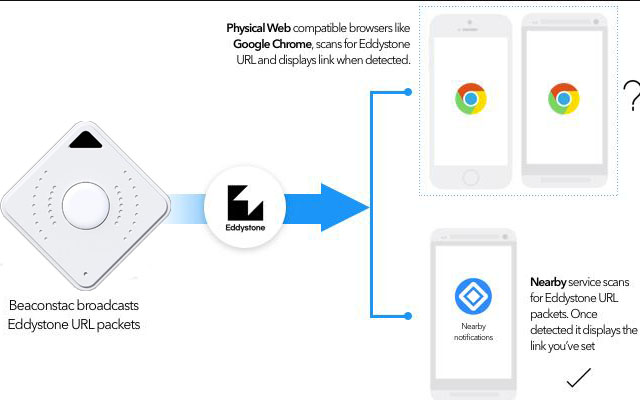
Beacon Technology-- Just How They Function And How They Can Be Utilized
Battle of the Sign Innovation: Google continues to deal with all-inclusive networking as well as has now introduced an equal to Apple's iBeacon. The open beacon style Eddystone uses a variety of devices as well as interfaces with which programmers can regulate the communication and also information exchange between various gadgets. The platform supports both Android and also iOS tools and is an all-natural sign innovation concept with extensions for UriBeacon/ Physical Internet, telemetry and sensor information, and also a central sign enrollment for open beacon systems. Specifications were published to the Github designer website. Google counts on the Bluetooth Low Energy transmission standard as well as small radio transmitters-- so-called beacons. With the help of the radio transmitter, it is feasible to attach the offline with the on the internet world. Traders can send item offers to the mobile phone of clients and also passers-by or utilize beacon technology for indoor navigating. So far, the setup of a matching application and the activation of Bluetooth was a prerequisite for utilizing signs. Google Sign Innovation You are a retailer and also have suggestions but not an app? Do you have an app however no iBeacon infrastructure? Contact MOKOSmart as well as we will certainly reveal you how you can profitably utilize the sign modern technology. Google has launched two interfaces as part of its beacon campaign: the Close-by API and also Proximity Beacon API. Close-by is meant to aid situate, connect as well as trade various tools in the location. Google counts on a mix of Bluetooth, Wi-fi, and also audio signals that are faint to the human ear. The Closeness Sign API can be made use of to control and manage the data traded in between the gadget as well as the signs. These are saved in the cloud. With the Places API, location-based actions can be controlled. Google is not only targeting the link of smart devices yet is also looking towards the wise home. Google deals with numerous sign suppliers, consisting of MOKOSmart, Estimote, Kontakt.io, and also Distance Networks. MOKOSmart sees Eddystone as "a vital step for all suppliers of proximity applications and beacon options" and also anticipates Google's significant effort to improve the beacon market and also hence likewise location-based solutions as well as applications. How do Sign tools function? MOKO Smart Bluetooth Beacon is based on BLE-- Bluetooth Low Energy. This enables a BLE-capable tool to start a so-called broadcasting procedure. It always sends the same worths at a fixed period, similar to a sign. With an iBeacon, the message sent, the supposed basic promotion, consists of UUID, major and minor. The mobile phone gets this special combination and can evaluate it without the requirement for pairing or data exchange. The variety of the BLE signal is up to 50m and hence closes a void in between NFC (Near Field Interaction), which sends information specifically yet just up to a few centimeters, and also Wi-Fi, which can cover a much longer range, and thus again is also imprecise for a set resolution. In the meantime, Google has followed up as well as published its very own procedure with Eddystone, which can contain even more details, such as a straight URL to allow making use of mobile internet applications. The basis of the beacons is the transmitter-receiver principle. For this function, transmitters (the signs) are put in the area that serves as signaling gadgets. These signs send signals in a certain time interval that the receivers (e.g. smartphones) can recognize as well as refine. This makes it simple to figure out the area of the recipient, which also allows interior navigating. Groups of the measured distance Depending upon the signal stamina, the determined range in between transmitter and receiver is separated right into among the following groups: The instant-- distance a few centimeters Near-- range a couple of meters Much-- distance as much as 70 meters A sign can send out a broadcast to the receiver if the receiver either goes into the area, "exited", or stays in the area (" lingered")-- depending upon how the sign was set up. These beacons can be set up using an administration platform from the maker. The gadget is registered to utilize the distinct identification number (UUID), major and minor of the beacon. Events can likewise be designated to the beacon. Monitoring platforms of beacons The signs only send their "identity" (UUID, Major, Minor). The associated app-- if the receiver is a smart device-- has to interpret this signal and also understand what to do with it. Nevertheless, the smart device just receives this signal when Bluetooth is triggered. Exactly how the application manages the details depend upon the application. The preferred activity (e.g. showing a press notice) is either implemented in the application itself or extra details are requested from a server. However, the information does not constantly need to be shown on the smartphone, however, motion patterns can also be taped and also later on assessed. An instance of this is the recording of sidewalks in stores, which can aid maximize shop formats. What are the advantages of Sign Modern technology? The innovation discussed and also the linked options make beacons especially amazing in location-based service: BLE can be used wherever you can not reach a sufficiently exact placement because GPS or Wi-Fi is not readily available with the precision you need, The technology can also be used where the range from NFC would certainly not be sufficient. Furthermore, signs send out signals to the individual's device with no action being called for, as holds with QR or AR codes, for instance, which the individual needs to capture with the camera. In the interior area, floorings are no more obstacles. This peculiarity utilizes the iBeacon procedure and also provides a "ranging", a loved one range dimension with "Immediate" says that you are just a couple of centimeters away, "Near" indicates a couple of meters, as well as "Far", implies greater than 10 m away from the sign, The applications of this modern technology appear practically endless: you can use loved one and absolute settings to the signs and therefore change whole branches of the market. Exactly how signs can be utilized? Beacon innovation has currently arrived in offline trade as well as is fiercely traded as a wonderful tool for the Robo (research online-- acquisition offline) instance. With the proper application, the smart device can utilize a beacon signal to recognize whether the user remains in the area of stores and also items that are of interest to him. Right here is a tiny example: Max sits on the sofa at night as well as takes a look at a new collection of winter season coats, consults with pals on social networks, and states which products he such as. A short time later on he remains on a buying road with a shop that uses this collection. The application registers the radio signals of the beacons behind-the-scenes and evaluates them: a push message educates Max that a layer can be acquired close-by and also sends him a price cut voucher. Max after that opens up the application. Via various other signs set up in his area, Max can see his placement on a map as well as the navigating path to the matching shop is presented. In the store, another press is activated on the worker's tablet that a potential consumer is on the method. She likewise educates him of the approximate time till it shows up. If Max already has a client account, the worker likewise learns Max's given name and also what product he is looking for-- the winter coat. When Max shows up, the seller can approach him and also speak to him personally, with the desired item in hand. If this seems acquainted to you: that's state-of-the-art in eCommerce. What are the areas of application? IoT Beacon technology can quickly be incorporated into daily life. The very first shopping mall in America is currently furnished with beacons. If a consumer enters the store geared up with beacons, he will certainly be educated about special offers, discount rates, as well as coupons, or he will be reminded of his birthday celebration voucher that has not yet been redeemed. If the consumer has conserved the shop's customer card in the connected application, it can already be opened at the checkout. Added item details, for example, the ingredients of a food, can additionally be presented in a supermarket. Another futuristic use case would be that in the future settlement for the purchase will certainly be made immediately when you leave the shop. For example, signs could be made use of as a good option to NFC in the mobile payment section. One more area of application can be discovered in the field of education and learning. As an example, signs can obstruct specific students' apps-- such as WhatsApp or Facebook-- or promptly block Web gain access to on their smartphones. Also, the presence of the trainees in the class could be inspected using beacons. Signs can likewise be utilized to support the family. As an example, if you approach the stove, the recipe book application opens. If you come close to the fridge, the shopping list opens. The opportunities for utilizing beacons are for that reason really wide. Final thought There are already many areas of application for signs that must make our every day lives easier and sustain common processes through automation. Using beacons is particularly interesting for the areas of advertising and marketing, marketing, interior navigation, and also mobile payment. Although this innovation is still in its early stage and also will continue to create in the coming years, some applications have already been carried out. It continues to be seen to what extent the trend with the signs will establish and also prove beneficial.

Beacon real estate provides you with benefits in many applications

Sign realty is a reasonably new idea that includes making use of Bluetooth signs genuine estate dealings. Bluetooth beacons are extremely little gadgets that run on BLE (Bluetooth Low Energy) technology. We can release Bluetooth signs for a range of objectives. However, they are really reliable genuine estate applications.
Advantages of Sign Real Estate
Send notices to potential customers when they are nearby
You can deploy Bluetooth beacons near the house you want to offer or near completion of the street. So, it will certainly trigger a notice when an individual strolls close by with a clever gadget. Nonetheless, for this to work, the smart tool must have Bluetooth. So, by doing this the customer can open up the notice on their smart gadget to find even more info connecting to the house. However, they can additionally execute more activities such as preparing a scenic tour. This is very beneficial for the property owners or the property representatives due to the fact that they will certainly recognize when the interested customer will certainly pass near your house. So, they can prepare and also advertise even more personalized web content that is tailored to that specific customer's needs.
The clients have improved access
If you want to sell a certain building then you don't have to worry about printing ads as well as posters any longer. You also do not have to set up building records as well as ask possible purchasers to undergo them throughout their sees. So, when you release mokosmart wearable beacon real estate, they deliver all the appropriate information to the smart tool of the potential customers during their excursions. Hence, a notification is sent out to the screen of the customer when he/she concerns take an excursion of the building. For that reason, they will come down on the info web page of that building when they click on that notification. For this reason, they have the ability to see more in-depth images as well as details.
Personalized boards and indications
Property owners like to utilize specialized sale indications and also boards for attracting the focus of prospective buyers Nevertheless, this strategy can become more effective when you deploy signs also. So, when a prospective customer strolls near the sale indication then it will immediately cause the relevant residential or commercial property details. It will certainly consist of details like the house location, construction material, and floor room. This way potential purchasers can register for alerts for a listing. So, a realty representative can then offer info for even more residences in the vicinity as per the preference of the customer.
Common advantage for vendors and purchasers.
The sign property can identify possible customers close-by and also ask to register by using the appropriate application or webpage. So, the vendors will understand about the customers coming to the residential or commercial property and also the buyers will have a better buying experience as compared to the conventional posters and adds. The buyers will certainly obtain welcome messages when they are available in your house. The real estate agents will certainly get notifications when a client comes to the property and they can embrace relevant courses of action.
Brand name understanding and brand acknowledgment
Sign realty can help homeowner by improving their brand name understanding. So, the customers will quickly recognize their brand name when they remain in the close-by location. On the other hand, vendors will certainly additionally obtain details regarding what kind of residential or commercial properties the clients want and also how many of them are visiting your home or sale. Thus, realty representatives can create an extra individualized buying experience for potential clients by deploying sign real estate modern technology.
Applications of Beacon Realty
The complying with are a few of the applications of sign real estate.
Introduce your open home event
You can use signs for sending out notifications to neighboring potential buyers that you are hosting an open residence occasion. So, by doing this you can bring in extra audiences as well as improve your conversion rate.
Bring in customers
Homeowner can make use of signs for sending notifications to neighboring people that your house is offer for sale. Therefore, even more people will certainly find out about it as well as even more clients will come forward.
Boost the sales funnel
Property representatives can develop a far better acquiring experience for prospective clients. Therefore, it will raise the possibilities of people in fact buying your house. Therefore, property agents will reinforce their sales funnel.
Use situations of Sign Property Service
In this section, we will certainly take a look at several of the use cases as well as exactly how you may benefit from them.
Makelaardij Hoekstra
It is a Dutch real estate firm that has four offices in different places. In order to improve their client involvement and lead generation, they made a decision to release Bluetooth signs. So, they had the ability to increase their promotions and also campaigns. Besides that, they received information regarding a potential customer when he was in a nearby area or if he wanted to schedule a check out to the home.
Redfin
It is a renowned realty firm and is located in Seattle. They made a decision to make use of Bluetooth beacons for reinforcing their proximity advertising initiatives. So, these signs sent notices of neighboring properties to customers and likewise prompted them to schedule a tour. In addition, they alerted the relevant sales agent whenever a customer revealed passion in checking out or purchasing the residential property. They included this details in making their sales approaches.
Spicerhaart
It is another popular real estate firm. Nonetheless, this set is located in the United Kingdom. They deployed beacon real estate in deluxe apartments so that when a buyer goes into, they receive a welcome message. So, they additionally obtained a notification for viewing the pertinent details of the apartment. The purchasers were likewise able to see an interactive as well as in-depth plan of the apartment so that the purchasing decision was simpler for them.
Sign Realty by MOKOSmart
If you are a homeowner or a realty representative then MOKOSmart is the most effective supplier for releasing your BLE beacons. We have a wide variety of beacon items that are matched for a variety of needs. Do not hesitate to call us if you require further details.

Untilization and Advantage of Standard PCB Panel Size
The PCB Panel advantage
A composite of published circuit card, i.e. Printed circuit boards that are not isolated are firmly repaired and also the setting up of the printed motherboard also comes from it, is typically taken as a published motherboard advantage. The charm of the design styles have to be the style of the published motherboard usage, in order to be able to utilize the published circuit card at optimum expenses and stocks and also arrangements. The impact of the PCB advantages on the production expenses of the PCB and the expense of assembly. The manufacturing expenses of published circuit boards become clear through the PCB panel examination control, which is the right law of the manufacturing panel with the control used by the printed circuit boards.
In the created instance in Figure 1, the lots on panel A (6-fold usage) is approx. 50% and also the lots on panel B (4-fold use) is approx. 70%.
With suitable individual printed circuit boards and also by skillfully dimensioning the panel and also preparing the panels appropriately, panel utilization of up to 85% can be achieved.
Number 1: PCB Panel use
pcb panel usage
Figure 2 reveals the family member expense payments in the production of printed motherboard for a conventional printed motherboard (100 * 160mm, 8 openings per cm2, 127µm track width/distance, surface area: HAL) depending upon the variety of layers. Essentially, only the costs for boring, cutting (racking up or milling), the electrical examination, packaging as well as for some material elements are straight depending on the number of printed circuit boards that can be suited on a panel. The continuing to be expense elements are independent of the number of printed motherboard per panel.
Figure 2: Expense elements in the production of printed circuit card
pcb parts
Normally speaking, it can be stated that approx. 70% to 80% of the PCB production costs are to be regarded as dealt with expenses, i.e. they are independent of the number of PCBs per panel. For the arrangements displayed in Number 1, this implies that the 8 circuit card (Panel B) can be made and also bought practically at the overall price of 6 circuit card (Panel A). The ideal advantage dimension in terms of producing prices is certainly dependent on the manufacturer. However, thinking about the commercially readily available panel cuts of 610 * 530mm or 1070 * 1225mm (typical sheet format) and the mounting margins and spacing needed for the manufacturing process, the PCB panel application and thus the price development in the PCB manufacturing for numerous PCB suppliers is an optimum advantage size of approx. 245 * 285mm.
The setting up process has cost components that are straight related to the number of parts per benefit as well as thus to the variety of printed motherboard per benefit, such as:
Intake of solder, direct SMD or THD setting up prices per element as well as AOI cost per part.
The expenses for packaging the circuit boards, an electric function test and for dividing the circuit card from the panel are symmetrical to the number of circuit boards in the panel. Other price elements are nearly independent of the number of printed motherboard in operation or the variety of parts on the published circuit card:
Throughput time of the benefit in the soldering system,
Time for paste printing,
The placement maker is idle throughout retraction/extension or adjustment of use.
Assembly prices for PCBs advantage
Figure 3: MOKO Printed Circuit Board Assembly expenses
pcb assembly
This decreases the processing costs in the PCB setting up for a benefit with an enhancing number of PCBs in the benefit, as displayed in concept in Figure 3. The following briefly analyzes whether taking full advantage of the number of published circuit card in terms of use is constantly highly sensible.
PCB Advantage Capacities
The optimum advantage size or PCB size differs depending upon the PCB maker and also technological tools. Based on the standard PCB panel size reduced 610 * 530mm, which is commonly processed, there are optimal dimensions of approx. 570 * 490mm for many producers. In electronic devices production at CAD-UL, the optimum dimensions are defined by the equipments made use of, supplied that it is to be carried out totally mechanically:
Paste printer 600 * 600mm
SMD choose and also put machine 400 * 550mm
Vapor phase soldering system 550 * 600mm
The following reasons oppose the processing of advantages with the optimum dimensions:
As PCB panel size boosts, this also loses stability, which can additionally be seen depending on the PCB thickness. There is a threat that the connection factors between the circuit card break because of incorrect handling.
The base materials for published circuit boards can diminish or extend throughout the published motherboard production procedure (dimensional stability). In addition, there are naturally manufacturing resistances in the manufacturing process of the circuit board, which can result in an offset of copper structuring, to boring and also contour of the circuit board as well as to a balanced out from layer to layer. With a lot of know-how and also by adjusting the manufacturing data, the PCB suppliers handle to keep the results to a minimum. With huge circuit boards or with large benefits where components with little pads, e.g. B. 0.4 mm pitch, positioned much apart, this can bring about borderline distinctions between the x, y placements of the pads on the circuit boards and also the connected outbreaks of the steel stencils for paste printing.
Extra actions have to be taken to prevent the bending of the PCB panels during transport in the transport gadgets, throughout paste printing, in the positioning system as well as throughout the soldering process. The flexing can result in faulty paste printing or mechanical stress on the solder joints.
In the manufacture of published circuit boards, troubles with the last assessment and also the electrical test emerge with raising measurements.
If there is a requirement not to permit failing motherboard in the panel, making best use of the variety of motherboard in the panel can result in a significant loss in return as well as hence to a price rise for the solitary motherboard.
Connection of the motherboard as well as benefit separation
The style of the advantages need to be reevaluated and also specified during the PCB layout stage to make sure that there are no surprises later throughout the assembly process. Generally, a choice for a treatment need to be made: scoring, milling or a mix of both. The setting as well as orientation of the components about the scraping trench or the milling ridges have to be picked so that the force used when the panels are divided is as tiny as possible. The copper needs to be set back adequately from the scoring trenches or perforation holes for the burrs to avoid water direct exposure. Ultimately, the design developer is additionally responsible for sufficient security of use during all machining processes and for the joint and coordinated optimization of the manufacturing and also setting up costs of the printed circuit card.
Connection of printed circuit boards as well as advantage splitting up for printed motherboard with a straight and continual shape with a minimum of two opposite parallel sides see Figure 4 and if there are no special needs when it come to border roughness, the scoring or notch milling process can be used. Trenches existing one over the various other are carved on both sides of the printed circuit card. The notch angle is normally 30 ˚, the notch depth depends upon the board thickness and the continuing to be core thickness is about 0.4 mm. The scribing process is no longer helpful for motherboard thicknesses above 2.0 mm. In order to reduce the mechanical anxiety when separating the published circuit boards from the panel to a minimum, CAD-UL utilizes a scratch PCB panel separator with a dealt with as well as a roller blade.
Number 4: PCB Rating advantages
For circuit card with uneven contours or if there are boosted demands concerning side roughness as well as dimensional precision, see Number 5, the circuit card shape need to be grated. The size of the milling cutters, normally 2.0 mm or 2.4 mm, for side processing must be defined due to the fact that the blanking procedure must be set to this milling size. Bars should stay throughout milling in order to connect the motherboard to each other or to the utility frame. The number, setting, as well as width of the internet must be thoroughly figured out depending upon the use or milling benefits of the published circuit board dimension and also density, in order to have the ability to assure adequate mechanical stability during all processing operations, along with to divide the published circuit card from the usage with little mechanical To be able to perform stress and anxiety on the solder joints and also parts. The internet can likewise be scratched or provided with perforation holes inside, on or outside the circuit board shape, see Figure 6, in order to be able to better decrease the anxiety impact when cutting.
Figure 5: PCB Milling advantages
With CAD-UL, the webs are either punched out by a pneumatically working web separator with a hook knife, or the circuit card are divided from each other by milling. Depending on the splitting up process and the placement of the opening openings, sharp-edged remnants of the internet can stay on the motherboard, which can lead to injuries. These are to be removed after the separation.
Number 6: Variations of router bars
A common feature of all depaneling procedures is that the circuit board flaws at the splitting up factors because of the mechanical activity throughout the separation which forces are exerted on the elements as well as the soldering points. These can cause component defects, in particular hairline fractures in SMD ceramic capacitors. Under particular situations, these issues are not instantly noticeable or have no result, yet just lead to breakdowns of the influenced elements after a long period of time.
Mixed benefits are specified as advantages that integrate different published motherboard with the same layer structure and similar production modern technology. The motivation for this is clear, published circuit card are only billed when and just one paste printing stencil is needed for a published motherboard with SMD on one side. If, nonetheless, the Gerber data collection provides several parts lists and several choice & area information sets for the benefit, in which reference names might be designated greater than as soon as, these information collections need to be incorporated with initiative and also risk of error by the job prep work department for electronic devices production in order to efficiently develop elements shopping and also to be able to successfully take into consideration the benefits as a setting up job. The majority of the moment, the various published motherboard are set up in the tool in one tool and these published circuit card are therefore required in the same number of items or in a set variety of pieces. Nonetheless, because raw circuit boards already stop working in use as well as mistakes can happen during the setting up of published circuit boards, the planned quantity proportion can not be ensured after the end of production. This can cause problems, especially with collection setting up. The savings in one-off costs at the start of the project may later be costly.
Figure 7: Combined benefit
All those entailed, the circuit board design, the motherboard supplier as well as the circuit card assembler ought to meticulously evaluate the benefits and also downsides of a mixed-use at the start of the task and also establish an ideal procedure with each other.
In order to make optimal use of the room on a manufacturing panel, it is additionally possible to utilize irregularly designed printed circuit card, e.g. L-shaped or T-shaped, to be arranged turned to each other on a PCB panel with 90 mit or 180 ˚. However, since published circuit card have preferred directions for paste printing as well as wave soldering, it ought to be checked whether this procedure likewise guarantees an optimum assembly process.
Lastly, a published circuit card that is to be produced and constructed separately, e.g. Elements put as well near the edge or where there disappears room for fiducial brand names as well as which therefore must be supplied with a receiving side on a minimum of 2 opposite sides are described as advantages
Please do not wait to call us if you have any type of questions concerning the design of the advantages or assistance in the creation of the advantages. Our staff members in the locations of PCB format and job preparation are constantly at your side with suggestions and also activity.
Dimensions of solitary motherboard as well as shipment benefits.
Single PCB
Please pick this choice if your circuit card contains a solitary circuit pattern. We always mill specific motherboard. The motherboard may contain interior cutouts as long as it does not separate the circuit layout. Otherwise, we speak of a PCB advantage.
If your PCB is smaller sized than 30x15mm, please put it in a shipment advantage. For this, we offer you the alternative "PCB Delivery advantage with on-line setup".
Distribution benefits
Distribution benefit from file or plan:
The same relates to multi-use if you want to get various conductor patterns in one usage.
Delivery advantages with online setup:
Do you have the data of a single circuit card as well as no advantage drawing, yet want to have your motherboard in the delivery benefit? After that just inform us in the configurator exactly how we can design the advantages. If you need fixed breaking openings, please bring them right into the single picture in advance.
You can locate a lot more on the definition of a shipment advantage in our tutorial!
Enrollment marks in the side of the sheet
On demand, we can introduce enrollment marks in the delivery location of your printed circuit boards. Put it like 3 copper pads with a diameter of 1.00 mm in the middle of the side of the PCB panel. In the solder mask, these are excused with 2.00 mm.
Bitter pills in the distribution benefit
In the delivery benefit, it can take place that individual circuit boards are set out by our quality control if the top quality does not meet our standard. We never repaint greater than 50% of the printed motherboard on a distribution advantage. We also fill in the missing variety of products by sending even more distribution advantages than you got. To ensure that you constantly get at the very least the wanted number at the end.
Features of flex PCB
A circumferential edge of ≥ 7.50 mm is definitely necessary. If there is a copper-free surface, the delivery benefit edge is always rostered onto the top and bottom. This protects against the PCB from bending. The edge of the delivery benefit is always covered on both sides with flex lacquer (even with a 1F structure).
General details on measurements
The dimension of your motherboard is determined by the measurement from center shape to facility shape. We, therefore, advise utilizing a contour line of 200 µm to prevent ambiguities.
At Moko Technology, your printed circuit card can be machined making use of notches, milling or a mix of notches as well as milling. We perform milled PCBs.
When grating a multiple-use, your published motherboard continues to be connected in the benefit by means of preserving bars. The basic cutters are 1.60 mm, 2.00 mm or 2.40 mm.
When notching, we put your published motherboard in the distribution benefit.

mokosmart contact tracing wearables
The entire world is undergoing a crisis as a result of the persistent COVID-19 and we desperately require call mapping if we are to take up reliable actions against it. In this regard, MOKO supplies you a variety of BLE-based sign items. These products are effective for call tracing, social distancing alerts, Individual Location, and so on. So, you can utilize these products for making certain security in your workplace and also for tracking crucial people in healthcare facilities.

moko PCB Assembly
Moko Technology Limited founded in the year 2006, is an expert at PCB Manufacturing and PCB assembly.
